| 2024 | 2025 |
Chronological record of the development and production of the implantable Blood Pressure Monitor (A3051).
[05-JUL-24] Our first run of A3050 circuits uses 1.2V as VCC for the programming connector. Our logic core power supply uses 1.2V but since its I/O banks are connected to VA we have to sever the track going to the programming connector and solder a wire link from VA to pin 1 of the programming connector. Using 1.2V as VCC resulted in us damaging multiple LCMX02-1200ZE logic chips; we note that the programming cable from the computer tries to pull VCC high and fails to program. We also note that the reference clock oscillator has its pads in the incorrect place causing its landing pattern to be incorrect. We will change this footprint on future layouts but will use an external function generator signal into a test pin for the time being.
[11-JUL-24] We load everything needed to power the A3051 board as well as the pressure sensor but nothing else on the circuit. We note that the pressure sensor consumes roughly 1.5 μA in its default state. We also note that pins IDY, SCL, and SDA are all at roughly 300mV. This implies that each of these pins has an internal pull-up resistor of 100 MΩs to its power supply. The pin SA0 on the other hand sits at roughly 2.7 V implying it has a 1 MΩ pull-up resistor to its power supply. These measurements were taken using a 10 MΩ oscilloscope probe.
[22-JUL-24] We find that our footprint for the pressure sensor is incorrect. Provided by the datasheet is a bottom view of the sensor, not a landing pattern for the footprint as we had initially thought. We design a new PCB with the correct sensor footprint, the correct oscillator footprint, and the correct voltage applied to VDD of the programming connector.
[22-NOV-24] We build an A3051A with our new A305101C printed circuit board. The programming connector now provides VA on P1-1. We drop C2 and C3 to 1 μF. We raise C1 to 22 μF. We are unable to program the logic chip unless we short U2-5 to U2-4. The voltage drop across U2 during programming otherwise drops VA to below 2.4 V and U3 cuts off the 1V2 supply to the logic chip. The oscillator footprint is still wrong: U6-3 has been exchanged for U6-1. We connect the two with a wire link so as to deliver RCK to U4. After programming, we can start the logic chip by shorting U2-5 to U2-4. Otherwise we see oscillations on VA with period 200 μs. We raise C3 to 22 μF, oscillations persist during power-up, although now with period 500 μs. Clean and dry. Connect power, jump-start with short from U2-4 to U2-5, now see RCK stable on TP1 and FHI on TP2. No VCO connected, nor sensor, but current is 128 μA for 128 SPS. Load MAX2524 and find DAC pins are in reverse order, so swap them in firmware. We are using commit 4340fb as a starting point. Load pressure sensor. After jump starting, TCK period is 198 ns. Reception 128 SPS, transmit value constant 32767. Current consumption now 135 μA.
We increase max_tcd in ROM.asm to 31. Our previous value of 15 was too low. Our U4 is speed grade 1, faster than the chip for which we chose the previous value. With value 15, the program decremented the divisor to zero, then went to 255, and dropped from there down to some value between 15 and 31. The calibration took about three seconds. Now it takes a fraction of a second. Our RF center frequency is 918 MHz, and TCK period is 207 ns from the calibration. Reception is poor. We observe VA to be dropping by 150-mV during transmission, which affects TUNE, on account of TUNE being derived from VA. We increase to C2 = C3 = 22 μF and reception is perfect. Drop to C2 = C3 = 10 μF and reception remains perfect. When we plug a CR2032 battery into the board, we do not need to jump start with C1 = C2 = 1 μF, but with 10 μF and 22 μF we do need to jump start.
No sensor interface yet: we are reading zeros from the disabled sensor interface, and transmitting them as 32767. But transmission is working without scatter, and current with sensor in standby looks good. Tag firmwarwe v2.1.
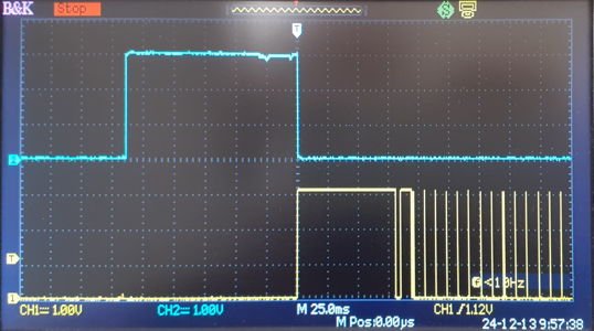
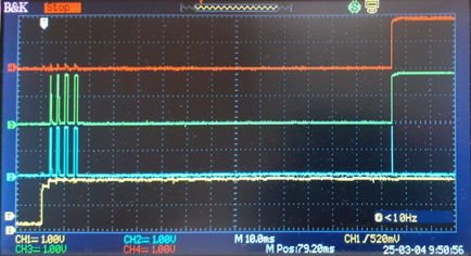
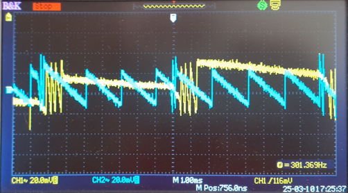
[23-NOV-24] With VB = 2.9 V and U3 = TPS70912, the A3051A circuit will not start up unless we jumper U2-4 to U2-5. The startup current passing through the internal resistance of U2 causes VA to drop below 2.4 V. We connect our A3051A directly to our bench-top power supply, with no ammeter, and obtain the following traces.
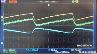
We load MCP1711T-12I for U3. This device is a pin-compatible micropower 1.2-V regulator, but it's maximum drop-out voltage at 50-mA is only 1.23 V, compared to 2.4 V for the TPS70912. Now the A3051A circuit powers up without any difficulty, see traces below.
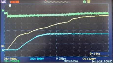
We place a 10-Ω resistor in series with our 2.9-V VB supply and obtain the above traces again, so as to measure the in-rush current at startup.
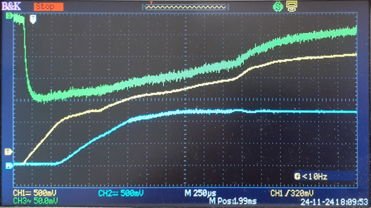
Our VB = 1.9 V drops by 200 mV with the 10-Ω series resistor, so our inrush current is 20 mA, relaxing to 5 mA in 4 ms. Quiescent current when powered up is 129 μA. In the P3051 firmware, we add PSCK, a 500-kHz clock to use with the I2C interface with the pressure sensor.
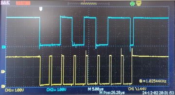
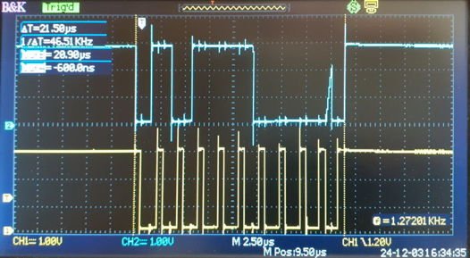
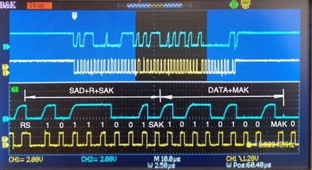
[02-DEC-24] We are studying the I2C interface of the LPS28DFW. The data sheet provides no complete waveforms. We present the four elemental tokens of the protocol below, as well as the complete byte write exchange.
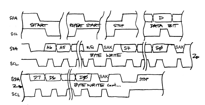
The Serial Data Access, SDA, line has a pull-up resistor. The Serial Clock, SCL, is always driven by the master either HI or LO. We refer to a positive pulse on SCL as a "clock pulse". The master transmits an ST token to begin the exchange. It transmits A6..A0 to select a sensor, and a zero-bit for WRITE. During each data bit transfer, the master drives SDA and then transmits a clock pulse. Once the seven bits have been transmitted, the master releases SDA and the slave should drive SDA LO. The master transmits a clock pulse, and during this clock pulse, SDA must remain LO. At the end of the clock pulse, the slave must release SDA. This transmission of a one-bit from slave to master is a slave acknowledgement, or SAK. After receiving the SAK, the master transmits the sensor's internal register address S7..S0. It reads another SAK bit and transmits eight data bits. It receives a final SAK, drives SDA LO, drives SCK HI, and releases SDA, to complete an SP token. This final release is the ST token. We can write multiple bytes to consecutive addresses by refraining from transmitting a ST token, and instead transmitting another eight data bits, waiting for another SAK, and repeating until we have transmitted as many bytes as we like, ending with an SP.
A read access begins with the same transmission of six sensor address bits, a write bit, a SAK, seven register location bits, which the data sheet calls SUB for "sub-address", and a second SAK. The access transforms into a read access by transmission of a repeat start token, RS, followed by the sensor address and a read bit. A SAK from the slave follows this eight-bit transmission, and now the master knows the slave is going to drive SDA during the eight subsequent clock pulses. The slave transmits D7..D0 and releases SDA. The master can now transmit a stop token, SP, to end the access. Or the master can indicate to the slave that it wants to read another byte, and this it does by transmitting a master acknowledgement, or MAK bit. The master drives SDA LO and transmits a clock pulse. The slave will now drive SDA during the eight subsequent clock pulses.
The maximum SCL frequency supported by the LPS28DFW is 1 MHz, with minimum SCL LO pulse length 0.5 μs and minimum HI pulse length 0.26 μs. The A3050's OSR8 microprocessor runs at 5 MHz in boost mode, so one SCL cycle is five clock cycles. We might be able to read out the sensor fast enough with instructions from the microprocessor, so we eliminate the Sensor Controller and Sensor Interface processes from our firmware and replace them with a bit-wise SDA and SCL interface, and write these bits separately with instruction cycles in a process known as bit-banging.
Our initial efforts produce an SCL period of 6.5 μs, which is 32.5 clock cycles. Looking at the code, we count 32 cycles. Bit frequency is 153 kHz. At this rate, a 16-bit read consisting of around 50 bits will take 300 μs, during which time the microprocessor will be running at 5 MHz in BOOST and consuming roughly 2.5 mA. At 128 SPS, we will be in boost for 330/7800 = 4.2% of the time and consuming 105 μA extra due to boost.
Instead of bit-banking, we consider "state-banging", where we have a register we can write to to generate a state of SDA and SCL. There are six states we are interested in for driving SDA and SCL. These are 00, 10, 01, 11, Z0, and Z1, where we have given two logic levels signifying SDA and SCL respectively for each state. If we denote bit seven of our accumulator as A, we could implement these with four locations: A0, A1, Z0, and Z1. We can now right eight bits in 80 clock cycles, assuming we have the eight bits in A to start with. Each bit is three writes to register plus a right-rotation. Our SCL period on writes is now only 2 μs. When reading bits, we can get the read bit into A0 with 13 clock cycles, but we somehow have to add the new bit to an accumulating byte. To do that we need another 12 cycles, making 25 in all. To read sixteen data bits we must transmit around 30 bits and read 20, for 800 cycles, or 160 μs.
[03-DEC-24] We are writing A7 to SDA, pulsing SCL, shifting A left, and so on, to transmit eight bits. We have the code in-line with no procedure calls. We have added four additional control registers to the sensor interface, those that implement 00, 01, 10, and 11. These save a little time, as we don't have to load any particular value into A when we write to the register.
We see sensor is driving SDA LO for an SAK during the ninth SCL pulse. When SCL goes LO, the sensor releases SDA, which begins its ascent to HI immediately, but is pulled down again 3 clock cycles later by the master. Current consumption is 130 μA, which is only slightly greater than the 128 μA we see with transmission. We add further byte exchanges until we compose a single-byte read from location 0x0F on the sensor, from which we read back the value 0xB4, which is correct. Current consumption is 145 μA.
[04-DEC-24] We remove the 10 and 11 tokens. The I2C protocol requires that no master or slave ever drives the SDA line HI. When we want to transmit a HI, we set SDA to Z instead of driving it HI, and trust that the pull-up resistor we have enabled on SDA in the logic chip will be sufficient to ensure a HI logic level by the time the master transmits a HI on SCL. From what we see in the above trace, the rise time of SDA with the pull-up resistor is about 500 ns.
We read the two bytes at 0x0F and 0x10. The first has a fixed value 0xB4. The second has a default value 0x00. We read the two bytes at 0x0E and 0x0F. The first has default 0x00. In both cases, we get the correct bits on oscilloscope, and receive them correctly by telemetry. Current consumption 151 μA.
We have deduced from examining the way the slave drives SDA that there is a delay between SCL going LO and the slave driving SDA LO, but the slave does not wait for the next SCL HI pulse before driving. We clock the slave data bit into a shift register on the rising edge of SCL. Whenever the master generates a Z1 token, it stores SDA. The slave appears to assert its value of SDA for 100 ns after the falling edge of SCL, so we could also use the falling edge of SCL.
Our assembler program runs fine with 987 bytes, but if we add nop instructions to increase to 1003 bytes, and the main loop no longer executes, and we see 1100 samples per second transmitted and received, with oscillating sample values.
[05-DEC-24] We route RESET to TP2 and RCK to TP1. We look at the power-up reset signal, which requires RCK to be running to be cleared. We connect our A3051A directly to our bench-top 3-V power supply.
The source of RCK is an SiT1553, for which the typical power-up time is 150 ms. Our code is running as we expect, with 987 bytes. We pad with NOPs to 1003 bytes. We see the same power-up reset, but code fails, transmitting 1058 SPS and consuming 650 μA. We include a pulse on TP2 = DF1 at the start of the initialization code, but this pulse is never generated. We remove the call to sensor_init, but initialization still does not run. We see pulses on DF0 generated by the interrupt routine. Restore call to sensor_init, pad code to 1067 bytes, still no initialization pulse on DF1. We add a loop at the start of our code that continuously generates a DF1 pulse. Our total code size is 1022 bytes. The loop works, generating the DF1 pulse. Move our initialization routine to the top of our code block, overwriting the loop. On start-up we should see a pulse of 0.3 ms on DF1. Instead the first pulse we see on DF1 is 3 ms, which is the pulse generated by sensor_init. In VHDL set TP2 = DF1, TP1 = (prog_addr=0). Now we see the 0.3-ms pulse on DF1 preceeded by TP1 falling LO. Later, we see the 3-ms pulse on DF1 from sensor initialization. We set TP2 = RESET, making no other changes to the code or software. We see the correct pulses.
We restore our code to the way we want it: a slow write to the control register on the sensor in sensor_init. We pad sensor_init until the total code length is 1003 bytes. We restore the initialize routine to its former position. With TP1 = DF0 and TP2 = DF1 we have the same failure of the code. But if we set TP1 = (prog_addr=0) the code works. We see a start-up pulse on DF1 for boot delay, then for sensor initialization, then repeated pulses for the main loop. We remove prog_cntr from the OSR8 and just use prog_addr. Code fails. We restore prog_cntr. Code fails. We see on TP1 that prog_addr is zero for 5-ns pulses, pulses of 450 ns, and for 60-μs pulses.
We have been jumping U2 with tweezers every time we program. Now we replace U2, but still have the same programming failure at VB = 3.0 V. We increase to VB = 3.3 V and programming is still unreliable. We remove U2 and jumper VA to VB. We reduce our code to 1000 bytes and it runs fine, reading the ID byte and zero, transmitting 128 SPS. Switch to reading TEMP_L and TEMP_H. We are writing 0x38 to IF_CTRL to specify 100 Hz update and averaging 4. Get zeros from these two registers. Current consumption is 263 μA. We try reading P_L and P_H for the pressure measurement. Still all zeros. Write 0x00 to IF_CTRL to return to one-shot mode. Go back to reading ID byte. Current drops to 156 μA and we see the 0xB4 (decimal 180) ID byte. Add three NOPs to the sensor_init routine, bringing code size up to 1003 bytes. Now see no startup pulses, but 600 SPS. We replace the logic chip, U4. Program with 1003-byte code, see same failure. Remove NOPs, size now 1000 bytes. Program, works as before. At 60°C current consumption is 360 μA. At −40 °C, 80 μA. At room temperature 160 μA.
[12-DEC-24] When the code works, we see prog_addr=0 asserted on TP1 for 130 ms after power-up. The firmware is asserting RESET until the RCK oscillator starts up.

After RESET, we have prog_addr<>0 for 85 ms. This we do not expect. We have DF1 LO, which means the CPU has not yet started the initialization routine. After 80 ms, the program counter returns to zero for 30 μs, which is one CPU clock cycle. Another 225 μs later TP2 goes high. That's 7.5 clock cycles, which is consistent with a jump (3 cycles), a load (2 cycles), a write to memory (3 cycles), and clocking the write on a falling edge of RCK. Thereafter, we have TP2 showing the behavior we expect from DF1, including pulses during interrupts.
Our hypothesis is that prog_addr is being set to some value in the range 1001-1003 when RESET is unasserted. So long as all entries in the program memory thereafter are NOPs, The program counter eventually wraps back to zero and our code executes correctly. The program memory is 4 KB, so that's 3k NOP instructions to go through, which should take 90 ms. We see 85±5 ms on our scope screen. But if the program address jumps to some other byte value, such as a RET instruction, the behavior of the CPU thereafter is chaotic.
[13-DEC-24] We examine the power-up process. We are resetting the ROM and RAM with RESET, which causes the program memory to be reset during the first instruction read. Thus the first instruction read from address zero is an nop instead of a jp_nn. This is the source of our start-up problems. When we disable the memory resets, we get a successful start-up.
[16-DEC-24] Our firmware is now stable. All case statements in the OSR8 have others clauses identical to definite clauses that complete the logic. The MMU in Main.vhd works with and without others clauses in the case statements, but the code is smaller with the others clauses included, so we leave them in place. We have 1018 byte code running.
We write 0x08 to address 0x10, which sets the sensor update rate to 1 Hz. We use our one-byte I2C write routine. We then read the temperature sensor's two-byte, two's compliment temperature measurement, which we divide by 100 to obtain the temperature. We use our two-byte I2C read routine. We obtain the following plots of cooling after heating the sensor with a soldering iron, and warming after being cooled with freezer spray.
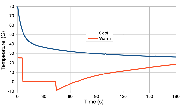
With our iron pressed on the side of the sensor, we are able to get the temperature measurement up to 110°C. We do not yet know the upper limit of the measurement. But the lower limit appears to be −10°C. At temperatures lower than −10°C, the sensor reads 0°C.
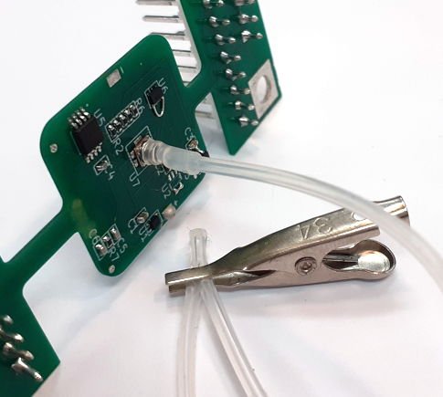
We fasten a silicone tube to the sensor with some heat shrink and seal with a clip at the end.
We configure by writing 0x38 to address 0x10. Now the update rate of the sensor should be 100 Hz. We start reading the top two bytes of the three-byte pressure measurement and transmitting on a second channel. We squeeze the silicone tube to generate variation in pressure. We have the pressure sensor on its default range, in which each LSB is 1/4096 hPa. We are reading out the top two bytes, so our telemetry counts are each 256 ÷ 4096 = 1/16 Pa. Current consumption is 280 μA at 25°C with two channels running at 128 SPS each, sensors updating at 100 Hz.
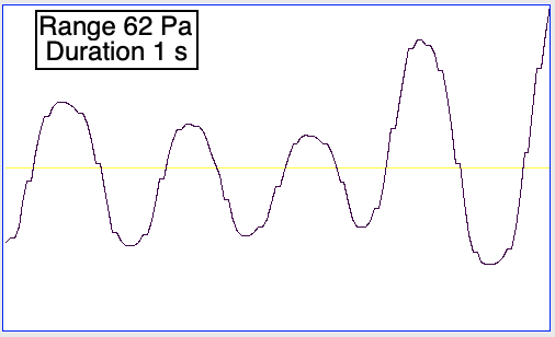
There are twenty-eight ledges in our waveform. These are the result of our reading out the pressure measurement 128 times per second, but the pressure is updated only 100 times per second. We now write 0x00 to 0x10 to switch to one-shot acquisition. We write 0x41 to 0x11 to initiate an acquisition with the larger 406 kPa range. Our telemetry counts are each 256 ÷ 2048 = 1/8 Pa. Atmospheric pressure gives a value of 8283 cnt, which is 103.5 kPa. According to the local weather station, barometric pressure in Waltham right now is 102.9 kPa.

The ledges are gone. Current consumption is 300 μA, suggesting a slope of around 0.7 μA/SPS. We remove temperature readout and transmission, 285 μA. We expand our sixteen-bit I2C read to twenty-four bits and read out the entire pressure measurement. We shift it one bit to the left, and use the top sixteen bits, so as to make a measurement with 1/16 Pa LSB and range 406 kPa. We open our tube and see 16506 cnt = 103.2 kPa. Current consumption 270 μA. We warm with our hands and current increases to 350μA. Assuming the current will be ≤400 μA in an animal, a CR2330 battery will give operating life at least 660 hrs = 28 days = 4 weeks.
[17-DEC-24] This morning, local barometric pressure is 101.7 kPa and our sensor says 101.4 kPa. We restore U2, which we had replaced with a wire link. We connect U3-1 directly to VB. We use VA as the enable for U3. The turn-on current from logic chip U4 now runs from VB through U3. Our circuit now turns on and off with a magnet. But we see the current jumping from 310 μA up to 2 mA at times, and often 500 μA. We see VA dropping. We are well familiar with the current drawn by the IO lines of U4, and by U5 and U6 from many other circuits. Our guess is that U7, the pressure sensor, is drawing the excessive turn-on current that U2 cannot deliver. Remove U2 and replace with wire link. Current is 270 μA at 128 SPS, roughly 20°C. The LPS28DFW data sheet says the sensor will work right down to VA = 1.7 V. We drop VB from 3.0 V, watching SDA. At 1.9 V the pressure sensor stops making new measurements. The pressure values remain fixed.
We restore temperature measurement, giving it 64 SPS, while pressure remains 128 SPS. The thermometer says the sensor is at 24.9°C. Current consumption is 280 μA. Codes size is 1637 bytes. We copy code from P3041 that updates a two-byte random number linear shift register. We use the bottom four bits of this register to offset the transmit moment. We observe transmission scatter on our oscilloscope.
At 25°C, the total current consumption of our A3050A is 280 μA. The LPS28DFW data sheet suggests the sensor's current consumption at 128 SPS will be around 100 μA. Transmission in SCTs consumes around 0.11 μA/SPS, and we are transmitting 196 SPS, so transmission accounts for 22 μA. The static current consumption of the logic chip is around 160 μA. Looking at the LCMXO2-1200ZE current consumption versus temperature we observed during development of the A3036, it appears that the logic chips we have been loading onto our A3051A exhibit worst-case current consumption. At 37°C we expect the consumption to rise to 250 μA, which will put our total consumption at 370 μA. An 80 mAhr CR1620 battery, the largest we can implant in a mouse, will run for only 9 days.
Our U2 cannot supply the start-up current demanded by the logic chip and sensor combined. Furthermore, our current consumption at 1.2 V limits mouse implant operating life to nine days. We propose deploying two ADP5301. One converts VB to 1V2 for the LCMXO2-1200ZE. The other converts VB to 1V8 = 1.8 V for digital I/O and the LPS28DFW. The VCO will be MAX2623 connected directly to VB and enabled by !SHDN driven high by the logic chip. When disabled, the VCO consumes only 10 nA. The converters are 90% efficient and consume only 7 μA quiescent in their "hysteresis mode". The output ripple on 1V2 in hysteresis is 40 mVpp. If we run the logic chip with 40 mVpp power supply ripple, our TCK clock period will fluctuate by ±6%, as we describe in D3037. During transmission, we propose to switch the converter to its "pulse width modulation" mode, in which the ripple is only 6 mVpp. In the PWM mode, the quiescent current of the converter increases to 500 μA. With the converter in PWM mode for 30 μs during each of 196 SPS the resulting increase in quiescent current due to using the PWM mode will be only 3 μA. For this extra 3 μA, our TCK frequency will be stable. We will no longer be relying upon U2 to supply current to the circuit as a power supply switch. We will use the logic output of U2 to drive the enable inputs on the two converters.
Assuming VB = 3.0 V, and setting 1V2 = 1.2 V, and accepting 90% efficiency, the 250-μA worste-case consumption of the logic chip at 37°C will draw 111 μA from the battery. The 100-μA drawn by the sensor from 1V8 = 1.8 V will be 67 μA. Transmit current remains 22 μA. Our total worst-case is 199 μA. Our minimum mouse-sized operating life is now seventeen days.
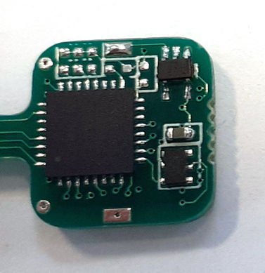
The converter version we prefer is the ADP5301ACBZ-1-R7, which permits 1.2 V and 1.8 V configuration and has an output discharge function. This function will ensure that the !SHDN input of the VCO is at 0V when the circuit is off. Price in quantity 100 is only $1.81. The logic chip could be the LCMXO2-1200ZE-1SG32I, a 5 mm × 5 mm QFN-32. These packages we can mount on a standard-spec, four-layer board by hand, and still have everything fit on a 12-mm square.
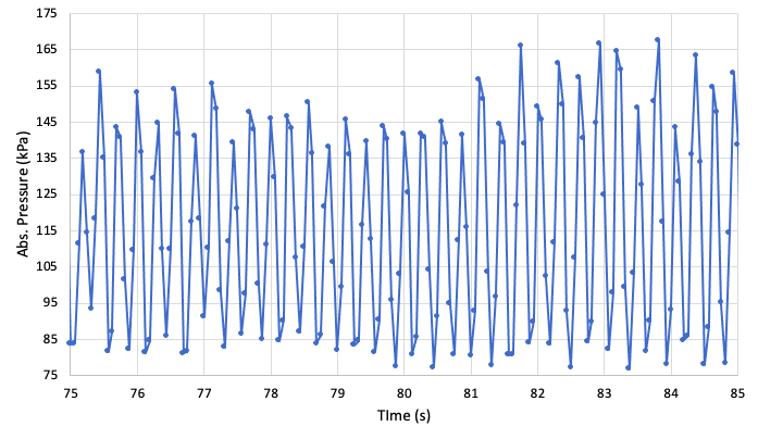
[08-JAN-25] With a 3-ml syringe attached to the silicone tube we have heat-shrinked to our pressure sensor, we generate 2-Hz pressure oscillations. The silicone tube is, however, expanding to a diameter of 10 mm, which complicates our efforts to calculate the actual pressure changes.
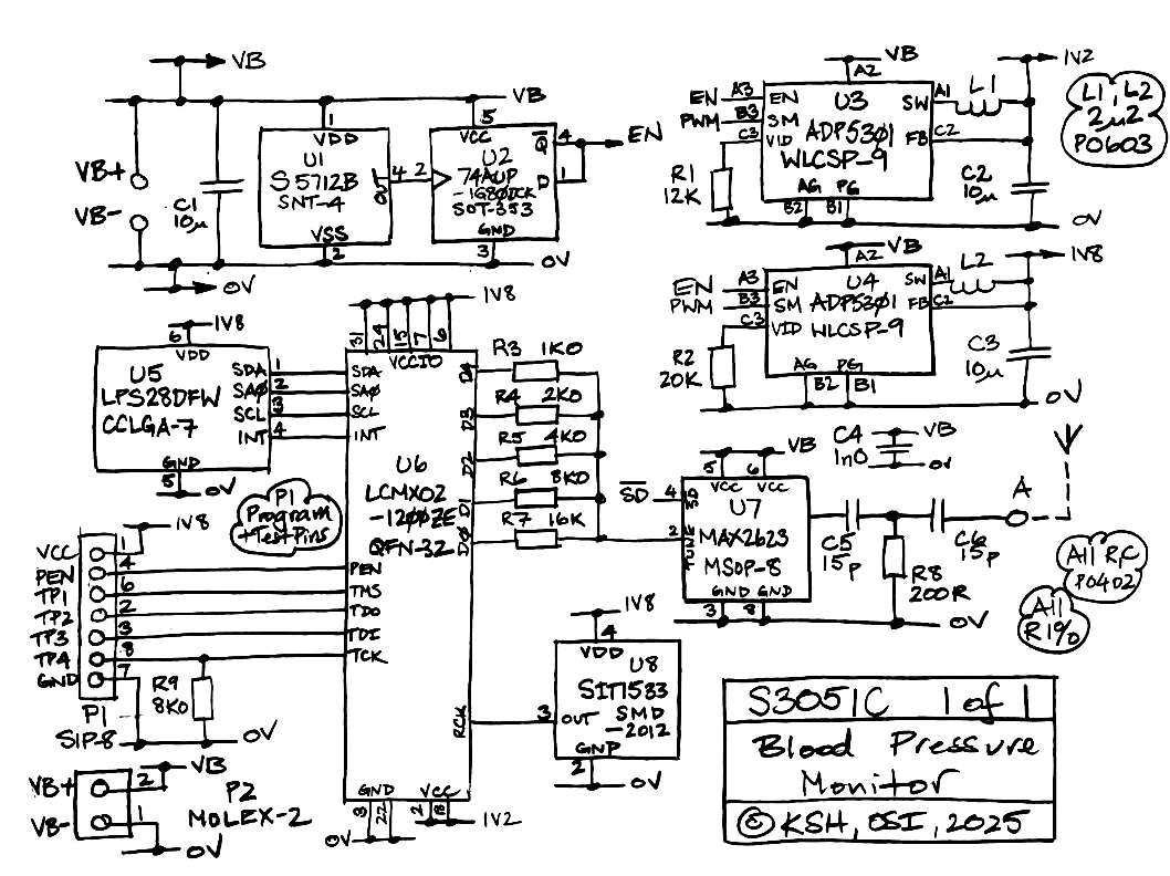
[09-JAN-25] Schematic for mouse-sized BPM with buck converters is S3051C_1. We will provide only one extension to the circuit board, and this will hold a SIP-8 for programming, which we will configure as test points after programming, giving us four test points on the same connector. A MOLEX-2 for power, a ground pad, and a pull-down resistor for TCK complete the extension.
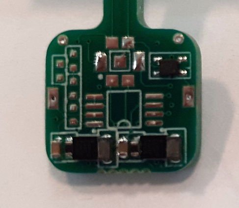
[13-JAN-25] Start work on A305101D, the mouse-sized printed circuit board for the A3051CV1 assembly. The outline is 12 mm rounded-square with 3-mm corner radius. We discuss with Kagan Agan and Aydan Agan of Duzce University and Rob Wykes of University College London a collaboration on testing the A3051B, a rat-sized version made to the A3051CV1 schematic, at the Duzce lab in the coming year.
[15-JAN-25] Calvin writes. "Here is my graph for the step testing of the blood pressure monitor as well as a graph I made today of oscillating air pressure measurements. From the step tests it seems that the sensor's pressure measurement is within 5 kPa of my calculated pressure for pressures up to like 40-50 kPa just by multiplying the digital signal by ADC to kPa conversion factor with no offset.

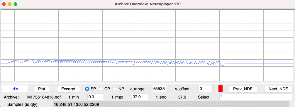
"I am able to get the oscillation graph by setting the Neuroplayer's interval to 0.0625 s, which is the smallest it will go and with which I get about four points per half period. With a 10-Hz oscillation presumably you would get only one or two points per half period which I think would be too few to be able to see the signal well. However, with the Overview feature the pattern can be seen better, but the signal is in ADC counts and not pressure.
[03-MAR-25] We have our A305101D boards. We load C1, U1, U2 and see the magnetic switch working. We load U3 and U4, which are WLCSP-9, along with their accompanying passives, and see 1V2 and 1V8 being created by the two buck converters. Their PWM inputs are floating and the power supplies have no load. Current consumption is 6 mA. Load U8, SIT1553, and U6, LCMXO2-1200ZE. The U6 QFN-32 package loads easily. Power up the board with the magnetic switch. Program the board with no difficulty. After programming, see about 500 μA with PWM = ENTCK. Reprogram with PWM = 0. Now see 150 μA at room temperature. We have the logic running its program, no VCO and no sensor.
[04-MAR-25] We have four test points on the A3050BV1 programming connector. We use them to show us the power-up signals USERSTDBY, STDBY and SFLAG. The first three are generated by our power-up process, the fourth is the answer from the LCMXO2 power-up controller saying that the chip has moved into standby.
We take another look at the power-up, in which we monitor the reference clock, RCK, which drives the power-up state machine. We see RCK does not start up for 155 ms after 1V8 is established, and only when it starts up do we see the power-up state machine entering standby. We set PWM to TXA (Transmit Active), so as to restrict its assertion to the transmission burts. Quiescent current is 153 μA. We examine the switching sides of L1 and L2 and see no switching during our 7-μs PWM pulses, but often a switching pulse will occur immediately after the pulse ends. We set PWM = 1. Current consumption is 7.1 mA. We put 1-kΩ resistors in parallel with C2 and C3. Current consumption is 9.0 μA. We set PWM = 0. Current consumption is 1.98 mA. We have 1.86 V on 1V8 and 1.22 V on 1V2. Our resistors are dissipating 4.95 mW. We are drawing 1.98 mA from 3.0 V, or 5.94 mW. According to the ADP5301 data sheet, the converter is 89% efficient at 1.2 V with a 3.0-V input and 1.2-mA load, and 93% efficient at 1.8 V and 1.8-mA load. We remove the resistor across C2, thus reducing the 1V2 current by 1.22 mA. Total current from VB drops to 1.40 mA. We remove 1.49 mW from 1V2 and see 1.74 mW reduction in input power. The 1V2 converter is operating at 86% efficiency. We replace the 1.0-kΩ across C3 with 33 kΩ. Total current from VB drops to 188 μA. We remove 3.35 mW from 1V8 and see a 3.63 mW reduction in input poer. The 1V8 converter is operating at 92% efficiency. Its remaining current is 30 μA, so this accounts for 20 μA of current from the battery. Where is the other 168 μA going? If it comes out of 1V2, the logic chip is drawing 504 μA. We turn on the PWM continuosly and see 7.54 mA. This current consumption is not consistent with the ADP5301 data sheet. Remove U4. Current drops to 1.63 mA. Load new U4, current 7.4 mA. Replace L2 with 3.3 μH, current 6.8 mA. Remove U4, connect 1V8 directly to VB, battery current 3.94 mA. Set PWM = 0, current 170 μA.
Start with fresh PCB. Load U1, U2, C2 and test. Load U4, L2, C3, and R2 = 12 kΩ. Pull PWM down with a wire. See 1V8 = 1.22 V, battery current 1.5 μA. See pulses on L2. Connect 1 kΩ in parallel with C3. See current 0.57 mA. We have 1.71 mW going in, 1.49 mW going into our load resistor, for 87% efficiency. Change R2 to 20 kΩ. Current 1.28 mA, 1V8 = 1.86 V, efficiency 90%. Tie PWM to VB. Current 5.0 mA. According to the ADP5301 data sheet, the quiescent current should be around 700 μA during PWM. Load U3, R1, L1, C2. Load 1.0 kΩ across C2. See 1.22 V on 1V2. Current 9.0 mA. Tie PWM to 0 V. Current 1.84 mA. Overall efficiency is 90%.
[05-MAR-25] Remove our two 1-kΩ load resistors. See 1.22 V and 1.86 V on 1V2 and 1V8 respectively. Total current is 1.5 μA. Turn off, current 0.9 μA. In hysteresis mode with no load, the two regulators are consuming only 0.6 μA together. Load U8 oscillator. This takes us a few tries. Current when on is 2.3 μA, when off is 0.9 μA.
[06-MAR-25] Load LCMXO2-1200ZE onto our second board. Program. See 177 μA flowing from battery. Assuming 90% efficiency converting 3.0 V to 1.22 V, we appear to have 400 μA flowing into our logic chip. We disable the microprocessor by connecting its clock to zero. We see 140 μA. Load working code, but disable the pull-up resistor on SDA and the pull-down resistor on IDY. See 164 μA. Restore resistors, program, see 165 μA.
[07-MAR-25] We remove buck converters from our No1 board. We wire 1V2 and 1V8 to VB. We apply bench power to VB through an ammeter and measure VB on the board with our oscilloscope. We power up the board with 1V2 = 1.2 V and our ammeter set to 200 mA. The logic chip enters standby mode and current consumption drops to around 280 μA. Now that the logic chip has entered standby mode, we measure current consumption for the range 0.975-1.27 V. We do not claim that 1.2 V is required for the board to enter standby mode. We merely noticed that we could not get the board to enter standby with our power supply at 1.0 V and the ammeter between the power supply and the logic chip. We will investigate the minimum voltage for successful power-up later. For now, we are interested in the variation of logic current versus core voltage.
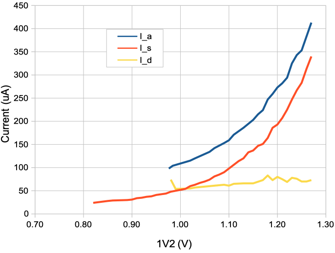
When provided by our buck regulator, 1V2 has an average value of 1.22 V and ripple of 40 mV. We expect current consumption to be around 300 μA. Our ADP5301 sets its output voltage when it powers up, by looking at the value of the feedback resistor. Our ADP5301ACBZ-1-R7 will generate 1.2 V, but nothing lower. We can generate 0.8, 0.9, 1.0, and 1.1 V with the ADP5301ACBZ-3-R7.
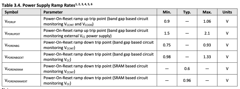
The table above suggests that we can always get the chip to power up at 1.06 V, and after entering standby, the chip will not turn itself off until 1V2 drops to around 0.6 V. If we set 1V2 to 1.1 V, we expect total current from 1V2 to be 160 μA. If our buck converter is 90% efficient converting 3.0 V to 1.1 V, we will draw only 65 μA from the battery at 25°C. Note that we previously saw battery current 140 μA with microprocessor disabled, 177 μA with processor running the BPM code. Our dynamic current consumption, which we do not expect to be a strong function of temperature or VCC, is (177-140) μA × 3.0 × ÷ 1.22 ÷ 90% = 100 μA. We must perform the same experiment with the disabled microprocessor to measure static power only.
The first circuit in which we used the LCMXO2-1200ZE was the A3030. The 1V2 power was provided by the TPS70912, with ±2% accuracy. Standby quiescent current was 57 μA. The A3037 used the ADP5301, which we see today producing 1.20-1.24 V. The A3041 used the MCP1711, ±20 mV. Some of the variation in quiescent current we observed beetween these assemblies may have been due to the values of VCC provided by their regulators.
[08-MAR-25] Repeat our current versus 1V2 measurement with the logic chip de-activated (CPU clock tied LO) and add to plot above. Subtract the two to obtain a measurement of dynamic current consumption. Program the logic to output !SFLAG on P1-8 so we can see when the chip enters standby without putting an ammeter in series with the power supply. We can get the logic chip to power up, configure, and go into standby provided the power supply voltage is at least 1.04 V. Return to No2 board with its 12 kΩ voltage control resistor. We see 1V2 = 1.23 V with ±20 mV ripple. We try R1 = 11.3 kΩ and 10.7 kΩ, but 1V2 remains unchanged. We try R1 = 10 kΩ and 1V2 contains spikes up to 2 V. The programming of the AD5301 output voltage is not analog, but threshold-based digital. We order some ADP5301ACBZ-3-R7.
[09-MAR-25] The ST1PS02DQTR is an adjustable, micropower buck regulator in a 2.0 mm x 1.7 mm TQFN-12 package. Its quiescent current is 0.5 μA. It is 80% efficient with 100 μA load, and it provides three digital inputs that adjust the output voltage during operation. By tying D1 = HI and D0 = LO, we allow D2 to control the output voltage, with D2 = LO generating 1.20 V and D2 = HI generating 1.0 V. Output ripple with a 2.2-μH inductor and 10-μA output current is 10 mV. With 10-mV output ripple, our ring oscillator frequency will be stable to ±1.5%. The 40-mV ripple of the ADP5301 dropped reception to 90% in the A3037 to 90%. We would be able to power up the logic at 1.2 V, then drop the voltage to a stable 1.0 V, at which point static current consumption from the logic will be only 50 μA at 25°C, drawing 1 V ÷ 3 V ÷ 80% × 50 μA = 21 μA. Static plus dynamic consumption for the A3051B would be 40 μA at 25°C and 60μA at 37°C.
[10-MAR-25] Add RF components to A3051BV1. We have omitted 1V8 connection to VCCIO for Bank 1 on U6-19. As a result, our D2 and D3 DAC outputs are disabled. Load a wire link from U6-19 to U6-15. With tx_frequency = 23 we have RF center at 917 MHz. Active current 96 μA. Despite adding RF transmission current, our active consumption has decreased. Assuming 22 μA as in A3051AV1 for RF transmit, our active logic current from the battery is now only 74 μA. Attach U5 pressure sensor. Pressure and temperature measurements working. We have a silicone tube fastened to the pressure sensor and we see pressure waves. The temperature is 26°C. Total current consumption 168 μA from 3.0 V. Reception is 98% from No51 pressure channel and 84% from No52 temperature. The logic's self-calibration of TCK seems to under-estimate the required divisor. We suspect this has something do with the 40-mVpp hysteresis in 1V2. We fix the calibration with transmit clock divisor set to 27. We now see 100% reception on No51 and No52 channels. Current from 3.0 V is 156 μA.
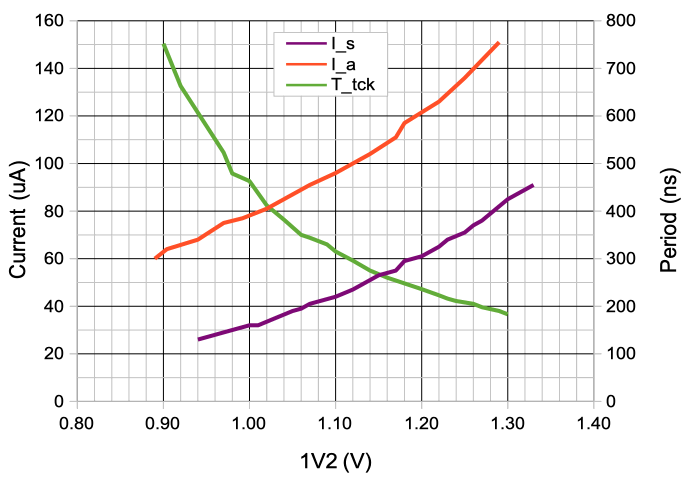
We destroy our No1 board logic chip by applying 3.0 V to its core. We replace and program. We have VCCIO for Bank 1 floating. Active current 200 μA at 1.20 V. Connect U6-19 to U6-31 with wire link, which provides 1V8 to VCCIO Bank 1. Active current at 1V2 = 1.20 V is 133 μA. Program with standby firmware. We must wire the board directly to our benchtop power supply and provide 1.3 V power to succeed in programming with the full clock speed. We disable temperature measurement, leaving 128 SPS of pressure, and measure active current versus 1V2. The active code runs until we get down to 1V2 = 0.88 V. We measure TCK period versus 1V2 voltage as well.
We program our No2 board with 128 SPS pressure. Active current is 148 μA from VB = 3.0 V at roughly 25°C. We have 1V2 = 1.22 V average. The logic chip is consuming 125 μA from 1V2, which appears as 125 μA × 1.22 ÷ 3.0 ÷ 90% = 56 μA at VB. If we drop 1V2 to 1.0 V, the 1V2 current will drop to 80 μA. At VB this will appear as 30 μA, saving us 26 μA and making the increase in current due to temperature negligible.
Our power supply ripple, caused by the hysteresis operation of the two buck regulators, is ±20 mV. There are two components to the hysteresis function. One is the 128 SPS drain of transmission, which causes the regulators to turn on. The other is the slower drain of standby current. In the case of 1V2 we have a 500-Hz ripple due to the standby current.
[11-MAR-25] We have the ADP5301ACBZ-3-R7 in hand. We take our No1 circuit and load these new regulators for U3 and U4. To load the BGA-9 package, we use iron at 600F with blob of solder resting on the top of the chip for 20 s, accompanied by tacky flux. We use 25 kΩ for R1 and R2, and C2 = C3 = 10 μF, L1 = L2 = 2.2 μH. We have our A3051B1 firmware loaded, 128 SPS pressure. We have no RF transmit nor the sensor, so we are going to see only the static plus dynamic logic current. We see 1V2 = 1.13±0.02 V, ripple frequency 200 Hz and 1V8 = 1.12±0.02 V, ripple 20 Hz. Current drawn from 3.0-V supply is 47 μA. Our previous measurements with this same logic chip and firmware suggest the total logic current is 100 μA. If so, our converter efficiency is 100 μA × 1.12 V ÷ 3.0 V ÷ 47 μA = 79% efficiency.
[12-MAR-25] We consider measuring respiration in a plethysmographic chamber direction with the LPS28DFW. We re-program our No2 board so the pressure dynamic range is 0-126 kPa instead of 0-406 kPa. The sensor's 24-bit output has 1 LSB = 100/4096 Pa = 0.024 Pa. We shift the 24-bit word one place left and transmit the top sixteen bits, so our BPM output has 1 LSB = 3.1 Pa. With stable pressure in our Faraday enclosure, pressure noise is 4 Pa rms. According to what we read online, the pressure resolution we need to measure respiration in a small-animal plethysmographic chamber is of order 1 Pa, with 0.1 Pa being preferred. The fluctuations in pressure are of order 10 Pa at most, and might be as small as 1 Pa. By taking the average of 16 measurements, we improve resolution to 1 Pa rms, but at this point we have only 16 SPS of pressure, and mouse respiration can reach 10 Hz. We conclude that the LPS28DFW might be able to measure respiration, but is not well-suited to the measurement.
We define the A3051A1 as 128 SPS pressure, 406 kPa range with CR1620 battery. We define the A3051B1 as 128 SPS pressure, 406 kPa range, 128 SPS temperature, and CR2330 battery. The A3051B1 current consumption is 166 μA at 25°C, so probably 200 μA at 37°C. The B1 will run for 55 days.